-->

ABOUT US

Our development agency is committed to providing you the best service.

OUR TEAM

The awesome people behind our brand ... and their life motto.

  • Kumar Atul Jaiswal

    Ethical Hacker

    Hacking is a Speed of Innovation And Technology with Romance.

  • Kumar Atul Jaiswal

    CEO Of Hacking Truth

    Loopholes are every major Security,Just need to Understand it well.

  • Kumar Atul Jaiswal

    Web Developer

    Techonology is the best way to Change Everything, like Mindset Goal.

OUR SKILLS

We pride ourselves with strong, flexible and top notch skills.

Marketing

Development 90%
Design 80%
Marketing 70%

Websites

Development 90%
Design 80%
Marketing 70%

PR

Development 90%
Design 80%
Marketing 70%

ACHIEVEMENTS

We help our clients integrate, analyze, and use their data to improve their business.

150

GREAT PROJECTS

300

HAPPY CLIENTS

650

COFFEES DRUNK

1568

FACEBOOK LIKES

STRATEGY & CREATIVITY

Phasellus iaculis dolor nec urna nullam. Vivamus mattis blandit porttitor nullam.

PORTFOLIO

We pride ourselves on bringing a fresh perspective and effective marketing to each project.

  • Pipelining in Computer Architecture


    Pipelining in Computer Architecture


    Parallel Processing


    A Parallel Processing system is able to perform concurrent data processing to achieve faster execution time.

    Example: While an instruction is being executed in the ALU, the next instruction can be read from memory.

    The system may have two or more ALUs and be able to execute two or more instructions at the same time. “So the purpose of
    parallel processing is to speedup the computer processing capabilities.”


    Pipelining Case: Laundry


    4 loads of laundry that need to washed, dried, and folded.

    – 30 minutes to wash, 40 min. to dry, and 20 min. to fold.
    – We have 1 washer, 1 dryer, and 1 folding station.


    What’s the most efficient way to get the 4 loads of laundry done?


    Pipelining in Computer Architecture


    Non Pipelined Laundry • Takes a total of 6 hours; nothing is done in parallel


    Pipelined Laundry • Using this method, the laundry would be done at 9:30.


    Pipelining in Computer Architecture


    Definition 

    Pipelining is an speed up technique where multiple instructions are overlapped in execution on a processor.


    Processors


    Computers, like laundry, typically perform the exact same steps for every  instruction:–


    • Fetch an instruction from memory
    • Decode the instruction
    • Execute the instruction
    • Read memory to get input
    • Write the result back to memory


    Instruction Pipeline


    Instruction execution process lends itself naturally to pipelining
    overlap the subtasks of instruction fetch, decode and execute

    • Fetch instruction (FI)
    • Decode instruction (DI)
    • Calculate operands (CO)
    • Fetch operands (FO)
    • Execute instructions (EI)
    • Write result (WR) Overlap these operations


    Instruction pipeline has six operations


    Instructions Fetch • The IF stage is responsible for obtaining the requested instruction from memory. The instruction and
    the program counter are stored in the register as temporary storage.

    Decode Instruction • The DI stage is responsible for decoding the instruction and sending out the various control lines to
    the other parts of the processor.

    Calculate Operands • The CO stage is where any calculations are performed. The main component in this stage is the ALU.
    The ALU is made up of arithmetic, logic and capabilities.

    Fetch Operands and Execute Instruction • The FO and EI stages are responsible for storing and loading values to and from memory.
    They also responsible for input and output from the processor respectively.

    Write Operands • The WO stage is responsible for writing the result of a calculation, memory access or input into
    the register file.


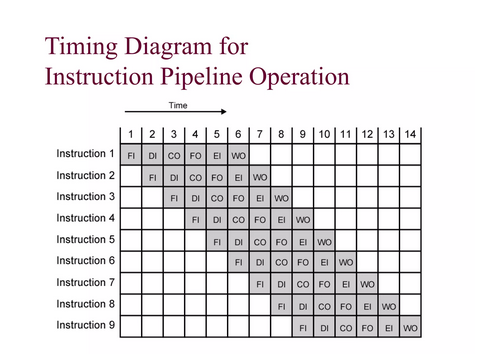
    Six Stage Instruction Pipeline


    Timing Diagram for Instruction Pipeline Operation


    Pipelining in Computer Architecture


    Pipelining in Computer Architecture


    Pipelining in Computer Architecture


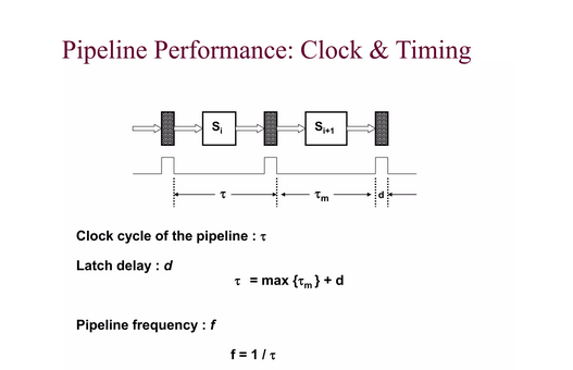
    Pipeline Performance: Clock & Timing Si Si+1  m d Clock cycle of the pipeline :  Latch delay : d  = max {m } + d Pipeline
    frequency : f f = 1 /  6


    Pipeline Performance: Speedup & Efficiency k-stage pipeline processes n tasks in k + (n-1) clock cycles: k cycles for the first task and n-1 cycles for the remaining n-1 tasks Total time to process n tasks Tk = [ k + (n-1)]

    For the non-pipelined processor T1 = n k Speedup factor Sk = T1 Tk = n k  [ k + (n-1)]  = n k k + (n-1) 7


    Advantages

    Pipelining makes efficient use of resources.
    Quicker time of execution of large number of instructions
    The parallelism is invisible to the programmer.


    Disclaimer


    All tutorials are for informational and educational purposes only and have been made using our own routers, servers, websites and other vulnerable free resources. we do not contain any illegal activity. We believe that ethical hacking, information security and cyber security should be familiar subjects to anyone using digital information and computers. Hacking Truth is against misuse of the information and we strongly suggest against it. Please regard the word hacking as ethical hacking or penetration testing every time this word is used. We do not promote, encourage, support or excite any illegal activity or hacking.


  • MySQL Transactions


    MySQL Transactions


    MySQL Transactions


    What are transactions?

    # Sequential group of DML statements, which is performed as if it were one single work unit.


    # Will never complete unless each individual operation within the group is sucessful.If any operation within the transaction fails, the entire transaction will fail.

    # Begins with the first executable SQL statement.

    # Ends when it is committed or rolled back, either explicitly with a COMMIT or ROLLBACK statement or implicitly when a DDL statement
    is issued.


    Sample Scenario


    Suppose a bank customer transfers money from his savings account (SB a/c) to his current account (CA a/c), the statement will be divided into four blocks:


    # Debit SB a/c
    # Credit CA a/c
    # Record in Transaction Journal.
    # End Transaction


    The SQL statement to debit SB a/c is as follows:

    UPDATE sb_accounts SET balance = balance - 500 WHERE account_no = 932656;


    The SQL statement to credit CA a/c is as follows:

    UPDATE ca_accounts SET balance = balance + 500 WHERE account_no = 933456;


    The SQL statement for recording in the transaction journal is as follows:

    INSERT INTO journal VALUES (100896, 'Transaction on Kumar Atul Jaiswal a/c', '28-NOV-11' 932656, 933456, 500);


    The SQL statement for End Transaction is as follows:


    COMMIT WORK;


    Ensures that all operations within the work unit are completed successfully; otherwise, the transaction is aborted at the point of failure and previous operations are rolled back to their former state.


    Disclaimer


    All tutorials are for informational and educational purposes only and have been made using our own routers, servers, websites and other vulnerable free resources. we do not contain any illegal activity. We believe that ethical hacking, information security and cyber security should be familiar subjects to anyone using digital information and computers. Hacking Truth is against misuse of the information and we strongly suggest against it. Please regard the word hacking as ethical hacking or penetration testing every time this word is used. We do not promote, encourage, support or excite any illegal activity or hacking.


  • Memory Subsystem in Computer Architecture


    Memory Subsystem


    Microcomputer Memory


    Memory is an essential component of the microcomputer system.
    It stores binary instructions and datum for the microcomputer.


    The memory is the place where the computer holds current programs and data that are in use. None technology is optimal in satisfying the memory requirements for a computer system.


    Computer memory exhibits perhaps the widest range of type, technology, organization, performance and cost of any feature of a computer system. The memory unit that communicates directly with the CPU is called main memory. Devices that provide backup storage are called auxiliary memory or secondary memory.


    Characteristics of memory systems


    • The memory system can be characterised with their Location, Capacity, Unit of transfer, Access method, Performance,
    • Physical type, Physical characteristics, Organisation.


    RAM, ROM, DRAM, Flash Memory


    • The main memory is a Random Access Memory. It is organized into words of fixed length.
    • The length of a word is called word length.
    • Each of these memory words has an independent address and each has the same number of bits.
    • Normally the total numbers of words in memory are some power of 2. Some typical memory word size are 8 bits, 16 bits, 32 bits etc.
    • The main memory can be both read and written into, therefore it is called read-write memory. 
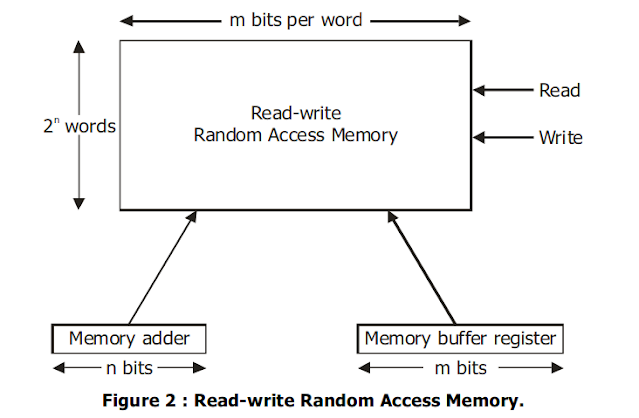
    • The block diagram of a read- write memory of RAM is shown in figure. 


    memory subsystem


    The access time and cycle time in RAM are constant and independent of the location accessed. The computer places the address of the location into which the data are to be read into the memory address register. This register consist of n binary devices (generally flip-flops), where 2n is the number of words that can be stored in the memory. Example : A 32 × 4 RAM means that this RAM has 32 words, 5 address lines (25 = 32), and 4 bit data word size.


    Dram (Dynamic Random Access Memory)


    RAM technology is divided into two technologies : Dynamic and Static. A Dynamic RAM (DRAM) is made with cells that store data as charge on capacitors. The presence and absence of charge on capacitor is interpreted as binary 0 or 1. Since the capacitors have natural tendency to discharge Dynamic RAM requires periodic charge refreshing to maintain data storage.


    ROM (Read-Only Memory)


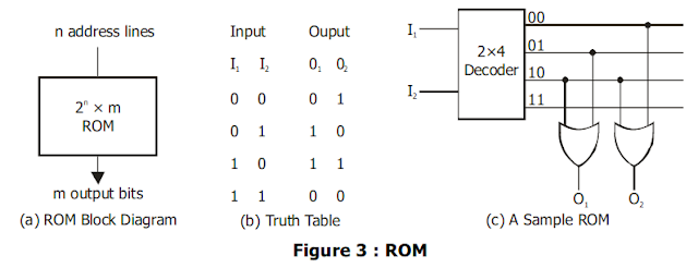
    A ROM is a memory or storage device in which a fixed set of binary information is stored. A ROM is a device with several input and output lines such that for each input value there is a unique output value. A block diagram of ROM is shown in the figure 3.


    It consist n input lines and m output lines. Each combination of the input variables in called an address. Each bit combination that comes out of
    the output lines in called a word. The number of bits per word is equal to the number of output lines m. The number of distinct address possible with n input
    variable is 2n.


    memory subsystem


    A ROM is characterized by the number of words (2n) and number of bits (m) per word. For example a 16 × 8 ROM which can be written as 24 × 8 consist of 16 words of 8 bit each, which mean there are 8 output lines and 16 distinct words stored in the unit. There are only 4 input lines because 16 = 24 and with 4 binary variable we can specify 16 address. A ROM is basically a combinational circuit and can be constructed as shown in figure 3 (c). On applying an Input I1 = 0, I2 = 0, the 00 line of the decoder is selected and we will get O1 = 0 and O2 = 1;
    on applying I1 = 0 and I2 = 1 we will get O1 = 1 and O2 = 0. The same logic is used for constructing larger ROM.


    Flash Memory :


    Flash Memory is a form of semiconductor memory which was first introduced
    in mid-1980. These memories can be reprogrammed at high speed and hence the
    name flash. These are electronic Random Access Memory but non-volatile in nature. 

    In flash memory the entire memory can be erased in a few seconds by using electric erasing technology. It is used in many I/O devices. It is also used to store data and programming algorithm in cell phones, digital cameras and MP3 music players. Basically flash memory falls in between EPROM and EEPROM.


    There are two kinds of flash memory :


    (i) Code storage flashmade by Intel, AMD, Atmel, etc. It stores
    programming algorithms and is largely found in cell phones 

    (ii) Data storage Flashmade by San Disk, Toshiba etc. It stores data and
    comes in digital cameras and MP3 players.


    Disclaimer


    All tutorials are for informational and educational purposes only and have been made using our own routers, servers, websites and other vulnerable free resources. we do not contain any illegal activity. We believe that ethical hacking, information security and cyber security should be familiar subjects to anyone using digital information and computers. Hacking Truth is against misuse of the information and we strongly suggest against it. Please regard the word hacking as ethical hacking or penetration testing every time this word is used. We do not promote, encourage, support or excite any illegal activity or hacking.


  • Hierarchy of Memory


    Hierarchy of Memory


    Hierarchy of Memory


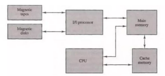
    Memory hierarchy Main Memory: memory unit that communicates directly with the CPU (RAM). Hierarchy of Memory


    Auxiliary Memory: device that provide backup storage (Disk Drives) Example of auxiliary memory: magnetic disks and tapes.  They are used for storing system programs, large data files, and other backup information  Only program programs and data currently needed by the processor reside in main memory.  All other information is stored in auxiliary memory and transferred to main memory when needed.


    Hierarchy of Memory


    Memory hierarchy system consists of all storage devices from the slow but high-capacity auxiliary memory to relatively faster main memory, to an even smaller and faster cache memory.

    Magnetic tapes used to store removable files and disks used as backup storage.  CPU communicates with auxiliary memory through I/O processor. 


    Cache Memory: special very-high-speed memory to increase the processing speed (Cache RAM)

    It is used to compensate the speed differential between main memory access time and processor logic.

    CPU logic is faster than main memory access.

    So small cache employed between CPU and main memory whose access time is close to processor logic clock cycle.

    So it is possible to increase the performance rate of the computer.

    As the storage capacity of the memory increases, the cost per bit for storing binary information decreases and the access time of the memory becomes longer.


    Example


    Auxiliary memory has a large storage capacity, is relatively inexpensive, but has low access speed compared to main memory.

    The cache memory is very small, relatively expensive, and has very high access speed.


    Goal of memory hierarchy


    To obtain the highest-possible average access speed while minimizing the total cost.


    Ratio


    Access time ratio between cache and main memory is about 1 to 7.


    For Example


    Cache memory may have an access time of 100ns, while main memory access time may be 700ns.

    Auxiliary memory average access time is usually 1000 times that of main memory.


    Block Size


    Block size in auxiliary memory typically ranges from 256 to 2048 words, while cache block size is typically from 1 to 16 words.


    Multiprogramming


    Multiprogramming refers to the existence of two or more programs in different parts of the memory hierarchy at the same time.

    For example, when one program is waiting for input or output transfer, there is another program ready to utilize the CPU.


    Memory management


    A program with its data normally resides in auxiliary memory. When the program or a segment of the program is to be executed, it is transferred to main memory to be executed by the CPU.  It is the task of the operating system to maintain in main memory a portion of this information that is currently active.
    3.  The part of the computer system that supervises the flow of information between auxiliary memory and main memory is called the memory management system.


    Disclaimer


    All tutorials are for informational and educational purposes only and have been made using our own routers, servers, websites and other vulnerable free resources. we do not contain any illegal activity. We believe that ethical hacking, information security and cyber security should be familiar subjects to anyone using digital information and computers. Hacking Truth is against misuse of the information and we strongly suggest against it. Please regard the word hacking as ethical hacking or penetration testing every time this word is used. We do not promote, encourage, support or excite any illegal activity or hacking.


  • Difference between RISC and CISC


    Difference between RISC and CISC


    What Is RISC?


    Reduction Instruction Set Computer (RISC) is a multiprocessor particularly designed to process limited computer instructions in order to operate at a much higher speed. On any given system, there are many programs and many instructions being executed. It was discovered that only 10% of all instructions were frequently executed, and that the other 90% clogged the pipeline, thus contributing to the system slowness.


    What Is CISC?


    Unlike the RISC model, Complex Instruction Set Computer (CISC) is a processor which is developed with a full (i.e. complex) set of instructions. The aim with this full instruction set is to provide the full processor capacity in the most efficient manner. RISC models proved, however, that better efficiency was achieved by reducing the set of instructions. 


    Difference between RISC and CISC


    RISC


    • Richer instruction set, some simple, some very complex.
    • Instructions generally take more than 1 clock to execute.
    • Instructions of a variable size.
    • Instruction interface with memory in multiple mechanism with complex addressing modes.
    • No pipelining
    • Upward compatibility with a family
    • Microcode control
    • Work well with simpler compiler.


    CISC


    • Simple primitive instructions and addressing modes.
    • Instructions execute in one clock cycle.
    • Uniformed length instructions and fixed instructions format.
    • Pipelining.
    • Instructions set is orthogonal (little overlapping of instructions functionality).
    • Hardwired control.
    • Complexity pushed to the compiler.


    Disclaimer


    All tutorials are for informational and educational purposes only and have been made using our own routers, servers, websites and other vulnerable free resources. we do not contain any illegal activity. We believe that ethical hacking, information security and cyber security should be familiar subjects to anyone using digital information and computers. Hacking Truth is against misuse of the information and we strongly suggest against it. Please regard the word hacking as ethical hacking or penetration testing every time this word is used. We do not promote, encourage, support or excite any illegal activity or hacking.


  • General Purpose Register


    What is a register?


    A register is one of a small set of data holding places that are part of a computer processor .


    A register may hold :

    a computer instruction
    a storage address
    or any kind of data (such as a bit sequence or individual characters)


    About Registers

    Rarely more than 64 registers in number.
    Small in size
    Typically a register is less than 64 bits in size


    General Purpose Registers Four general-purpose registers:

    1. AX
    2. BX
    3. CX
    4. DX


    AX (Accumulator)


    This is accumulator register. It is of 16 bits and is divided into two 8-bit registers AH and AL to also perform 8-bit instructions. It is used in arithmetic, logic and data transfer instructions in 8086 microprocessors. In manipulation and division, one of the numbers involved must be in AX or AL.


    BX (Base Register)


    This is the base register. It is of 16 bits and is divided into two 8-bit registers BH and BL. BX register is an address register. It usually contains a data pointer used for based, based indexed or register indirect addressing.


    CX (Count register)


    This is Count register. It is of 16 bits and is divided into two 8-bit registers CH and CL to also perform 8-bit instructions. This serves as a loop counter. Program loop constructions are facilitated by it. Count register can also be used as a counter in string manipulation and shift/rotate instruction.    


    DX (Data Register)


    This is data register. It is of 16 bits and is divided into two 8-bit registers DH and DL to also perform 8-bit instructions. Data register can be used as a port number in I/O operations. It is also used in multiplication and division.    


    SP (Stack Pointer)


    This is stack pointer register pointing to program stack. It is used in conjunction with SS for accessing the stack segment.  It is of 16 bits. It points to the topmost item of the stack. If the stack is empty the stack pointer will be (FFFE)H. Its offset address is relative to the stack segment.


    BP (Base Pointer)


    This is base pointer register pointing to data in stack segment. Unlike SP, we can use BP to access data in the other segments. It is of 16 bits. It is primarily used in accessing parameters passed by the stack. Its offset address is relative to the stack segment.


    SI (Source Index)


    This is source index register which is used to point to memory locations in the data segment addressed by DS. Thus, when we increment the contents of SI, we can easily access consecutive memory locations.  It is of 16 bits. Its offset is relative to the data segment.


    DI (Destination Index)


    This is destination index register performs the same function as SI. There is a class of instructions called string operations, that use DI to access the memory locations addressed by ES.


    Disclaimer


    All tutorials are for informational and educational purposes only and have been made using our own routers, servers, websites and other vulnerable free resources. we do not contain any illegal activity. We believe that ethical hacking, information security and cyber security should be familiar subjects to anyone using digital information and computers. Hacking Truth is against misuse of the information and we strongly suggest against it. Please regard the word hacking as ethical hacking or penetration testing every time this word is used. We do not promote, encourage, support or excite any illegal activity or hacking.


  • Ranchi University HTML Mid Sem Exam Paper with solution

     
    Ranchi University HTML Mid Sem Exam Paper with solution


    Group A


    1. <h6></h6> 

    2. <!DOCTYPE html>

    3. <!-- -->

    4. break the line

    5. meta


    Group B


    2. Design a login web page using HTML and CSS.


    <!DOCTYPE html>
    <html>
    <head>
    <title>Login Form</title>
    
    <style>
    
    body {
    	background: linear-gradient(to right, #1e5799 0%, #3ccdbb 20%, #16c9f6 100%);
    	
    }
    
    .form-css
    {
    	top: 50%;
    	left: 50%;
    	transform: translate(-50%, -50%);
    	position: absolute;
    	background-color: white;
    	border: 2px solid black;
    	border-radius: 20px;
    	padding: 50px;
    }
    
    
    .avatar-image img
    {
    	 justify-content: center;
    	 top: 0%;
    	 left: 50%;
    	 transform: translate(-0%, -50%);
    	position: absolute;
    	border: 1px solid black;
        border-radius: 50%;	
    	
    }
    
    button {
    	font-family: sans-serif;
    	padding: 5px;
    	cursor: pointer;
    }
    
    
    </style>


    </head>
    
    <body>
    <div class="container">
    
    <form action="controller/login-db.php" method="POST" class="form-css">
    <div class="avatar-image">
    <img src="image/avatar.png"  alt="avatar">
    </div>
    <br />
    <br />
    Email ID :
    <input type="text" name="email" placeholder="Enter your Email ID">
    <br />
    <br />
    Password :
    <input type="text" name="password" placeholder="Enter your password">
    <br />
    <br />
    <button type="submit" name="submit">Login</button>
    <br />
    <br />
    <a href="Signup.php">Signup Here</a>
    </form>
    </div>
    
    </body>
    </html>


    Ranchi University HTML Mid Sem Exam Paper with solution


    updating...


    Disclaimer


    All tutorials are for informational and educational purposes only and have been made using our own routers, servers, websites and other vulnerable free resources. we do not contain any illegal activity. We believe that ethical hacking, information security and cyber security should be familiar subjects to anyone using digital information and computers. Hacking Truth is against misuse of the information and we strongly suggest against it. Please regard the word hacking as ethical hacking or penetration testing every time this word is used. We do not promote, encourage, support or excite any illegal activity or hacking.


  • WHAT WE DO

    We've been developing corporate tailored services for clients for 30 years.

    CONTACT US

    For enquiries you can contact us in several different ways. Contact details are below.

    Hacking Truth.in

    • Street :Road Street 00
    • Person :Person
    • Phone :+045 123 755 755
    • Country :POLAND
    • Email :contact@heaven.com

    Lorem ipsum dolor sit amet, consectetur adipisicing elit, sed do eiusmod tempor incididunt ut labore et dolore magna aliqua.

    Lorem ipsum dolor sit amet, consectetur adipisicing elit, sed do eiusmod tempor incididunt ut labore et dolore magna aliqua. Ut enim ad minim veniam, quis nostrud exercitation.